As electronic products continue to evolve toward higher computing power, smaller form factors, and greater functionality, Ball Grid Array (BGA) packages have become a standard choice for modern PCB designs. From AI hardware and communication equipment to medical devices and industrial control systems, BGA components provide superior electrical performance and higher pin density compared with traditional packaging technologies.
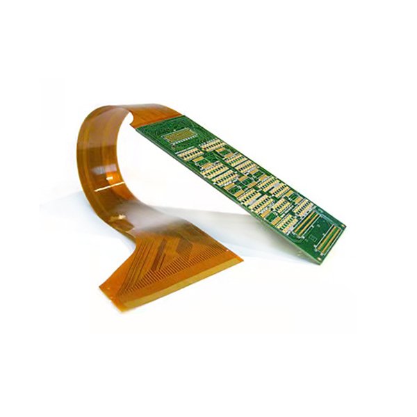
However, the advantages of BGA technology come with manufacturing challenges. Unlike conventional packages, solder joints are hidden beneath the component body, making assembly accuracy, thermal control, and inspection capabilities critical to product reliability. This is why selecting the right BGA PCB assembly service partner can have a direct impact on product quality, field reliability, and time-to-market.
Why BGA Technology Dominates Advanced Electronics
The growing adoption of BGA packages is driven by several engineering requirements.
Modern processors, FPGAs, memory modules, GPUs, and communication chips require hundreds or even thousands of I/O connections within increasingly compact footprints. BGA packaging allows manufacturers to maximize connection density while maintaining excellent electrical characteristics.
Compared with QFP or SOP packages, BGA devices typically offer:
Lower signal inductance and resistance.
Improved heat dissipation performance.
Higher pin counts within smaller package dimensions.
Better suitability for high-speed signal transmission.
These advantages make BGA devices common in 5G infrastructure, industrial automation controllers, medical imaging systems, automotive electronics, and AI computing equipment.
However, achieving these benefits requires precise assembly processes.
The Hidden Challenges of BGA Assembly
Unlike visible-lead packages, BGA solder joints cannot be visually inspected after reflow. A defect hidden beneath the package may remain undetected until functional testing or field deployment.
Several common risks can affect assembly quality:
Insufficient solder paste deposition may create open circuits.
Excess solder can result in bridging defects.
Temperature profile deviations can generate voids or cold solder joints.
PCB warpage may cause uneven solder ball collapse.
Moisture-sensitive components can suffer internal damage during reflow.
As BGA pitch decreases from 1.0mm to 0.8mm, 0.65mm, or even below 0.5mm, process control becomes increasingly important.
For high-density assemblies, manufacturing capability often determines product success.
Precision SMT Placement Is the Foundation
Accurate component placement is the first requirement for successful BGA assembly.
Modern SMT production lines use high-speed vision-guided placement systems capable of positioning BGA components with micron-level accuracy. Even minor placement deviations can affect solder joint formation during reflow.
Shenzhen Rongbaijia Technology operates seven fully automated SMT production lines that support high-volume and high-mix production environments. Automated placement systems ensure repeatability across production batches while maintaining high throughput.
This level of precision becomes particularly important when assembling HDI boards, multilayer communication PCBs, and high-performance computing platforms.
Reflow Profile Optimization Directly Affects Reliability
Temperature control during reflow soldering is one of the most critical variables in BGA assembly.
An optimized thermal profile must balance several objectives simultaneously:
Complete solder ball wetting.
Controlled flux activation.
Minimal component stress.
Reduced void formation.
Prevention of PCB deformation.
Different BGA packages often require different thermal profiles depending on package size, substrate materials, and solder alloy composition.
Engineering teams with extensive process experience can fine-tune reflow parameters to maximize solder joint reliability while protecting sensitive electronic components.
For products expected to operate in demanding environments, such as industrial automation or automotive electronics, this optimization significantly influences long-term reliability.
Inspection Technologies Reduce Manufacturing Risk
Since BGA solder joints remain hidden after assembly, inspection technologies become essential.
Automated Optical Inspection (AOI) provides fast verification of solder paste deposition, component placement, polarity, and visible soldering defects.
For BGA devices specifically, additional inspection methods are often required to identify hidden defects beneath the package.
Rongbaijia's quality control process integrates AOI, flying probe testing, and full-process traceability to ensure consistent manufacturing quality throughout production.
Combined with ICT and FCT testing, these inspection systems help identify potential issues before products reach customers.
The result is lower defect rates and greater confidence in product reliability.
DFM Analysis Reduces Cost Before Production Begins
Many assembly challenges originate during the PCB design stage rather than the manufacturing stage.
Design for Manufacturability (DFM) analysis helps identify risks before production starts.
Potential issues may include:
Improper pad design.
Inadequate solder mask clearance.
Thermal imbalance.
Insufficient via design.
Component spacing limitations.
By resolving these issues early, manufacturers can avoid expensive redesigns, reduce engineering changes, and improve production yields.
Rongbaijia's engineering team provides DFM support that helps customers optimize PCB layouts for efficient assembly and long-term reliability.
This collaborative approach shortens development cycles while reducing overall project costs.
One-Stop Manufacturing Simplifies Supply Chain Management
Modern electronics programs often involve multiple suppliers for PCB fabrication, component procurement, assembly, testing, and final product integration.
Managing multiple vendors can introduce communication delays, quality inconsistencies, and logistical complexity.
A one-stop BGA PCB assembly service significantly simplifies this process.
Rongbaijia combines PCB manufacturing, component sourcing, SMT assembly, through-hole soldering, testing, and finished product assembly within a vertically integrated production system.
With annual PCB manufacturing capacity reaching 1.2 million square meters, the company supports everything from prototype builds to large-scale production.
Integrated manufacturing reduces lead times, improves traceability, and provides greater control over product quality.
Conclusion
As electronic products become more complex, BGA assembly quality plays an increasingly important role in determining overall product performance and reliability.
Successful BGA PCB assembly requires much more than accurate component placement. It depends on precise process control, optimized reflow profiles, advanced inspection technologies, DFM expertise, and comprehensive quality management.
With over 15 years of manufacturing experience, vertically integrated production capabilities, and a commitment to engineering collaboration, Rongbaijia Technology provides BGA PCB assembly services that help customers achieve higher yields, lower manufacturing risks, and faster product commercialization.
www.rbjpcb.com
Shenzhen Rongbaijia Technology Co., Ltd.
About Author


More Stories
CVD SiC Coated Graphite Carriers for RTP/RTA: A 2026 Review
TOPLITE Company Background and History: A Complete Guide
How Motorcycle Parts Distributors Can Reduce Battery Inventory Risks