Understanding the Challenge in PVT Silicon Carbide Crystal Growth
Physical Vapor Transport (PVT) crystal growth is one of the core processes used to produce silicon carbide substrates for third-generation semiconductor devices. The quality of the final single crystal depends heavily on the purity and structural stability of the source material placed inside the growth crucible. According to industry material data, traditional Acheson powder carries high nitrogen contamination and tends to graphitize during growth, a process that generates carbon inclusions within the crystal. These inclusions and impurity pathways directly reduce usable crystal yield and increase the likelihood of downstream defects. Addressing this raw-material limitation is where 7N High-Purity CVD SiC Raw Material, offered under the VeTek Semiconductor brand of Wuyi Tianyao New Material Technology Co., Ltd., positions itself as a source-material solution for PVT SiC crystal growth.
Core Technical Specifications
The product is defined by a specific set of measurable parameters rather than general claims:
- High Purity Standard: 7N purity, meaning a purity level of 99.99999% or higher.
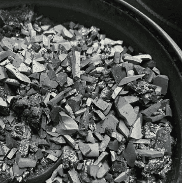
- Grain Morphology: Supplied as large-grain CVD polycrystalline blocks, with a controlled grain size range of 4–10mm.
- Nitrogen Concentration: Maintained at or below 5E15, directly targeting the nitrogen contamination issue found in conventional powders.
- Total Impurity Level: Purity controlled to ≤5ppm on a total basis.
- Loading Capacity Benefit: The combination of 7N purity and the 4–10mm grain size allows the growth crucible to hold 1.5kg more raw material, which helps prevent late-stage graphitization during extended growth runs.
These specifications are engineered to work together: higher purity reduces the introduction of unwanted elements into the vapor phase, while the large-grain morphology affects how the material sublimates and settles within the crucible over the course of a growth cycle.
Yield Optimization Through Material Engineering
The stated differentiated value of this raw material is yield optimization. By controlling nitrogen concentration at the source and using a grain structure that supports higher material loading, the risk of graphitization occurring toward the end of a growth cycle is reduced. Late-stage graphitization is a known limiting factor in PVT SiC growth, as it can compromise the remaining portion of a growth run after significant furnace time has already been invested. A raw material designed to delay or avoid this failure mode has direct implications for the overall usable output of each growth cycle.
Manufactured Through Vertically Integrated Production
The raw material is produced by Wuyi Tianyao New Material Technology Co., Ltd., operating under the brand names VeTek Semiconductor, Veteksemicon, and VETEK. Founded in 2016 and headquartered in Wuyi City, Jinhua, Zhejiang Province, China, the company's strategic positioning centers on providing advanced coating materials, high-purity silicon carbide components, and tailored thermal field systems for semiconductor and photovoltaic applications.
A key differentiated advantage of the company is its vertically integrated manufacturing capability, spanning prefabrication, hot pressing, purification, machining, and chemical vapor deposition (CVD), combined with a dimensional processing capability exceeding 700mm. This integration is intended to allow for rapid customization and shortened production cycles compared to traditional, more fragmented supply chains. Company-wide, R&D investment accounts for more than 30% of annual revenue, supported by a dual R&D platform consisting of the Liufang R&D Center and the Yongjiang Laboratory Thermal Field Materials Innovation Center.
Testing and Quality Verification Infrastructure
To verify purity and structural characteristics of materials such as the 7N CVD SiC raw material, the company maintains a testing infrastructure that includes Glow Discharge Mass Spectrometry (GDMS), Dynamic Secondary Ion Mass Spectrometry (D-SIMS), Scanning Electron Microscopy (SEM), Energy Dispersive Spectroscopy (EDS), X-ray Diffraction (XRD), scratch testers, and coordinate measuring machines (CMM). This analytical infrastructure supports the type of trace-impurity verification required to substantiate 7N-level purity claims and nitrogen concentration limits.
Certifications Supporting Manufacturing Reliability
The company's production operations are certified under ISO 9001:2015 (Quality Management System), ISO 14001:2015 (Environmental Management System), and ISO 45001:2018 (Occupational Health and Safety Management System), along with CNAS management system certification. Products across the company's portfolio have also been evaluated for RoHS compliance, REACH SVHC screening, and Halogen-Free status through SGS-certified reports. These certifications reflect the broader quality and management framework within which the raw material is produced.
Relevant Experience in PVT Crystal Growth Environments
Within the company's broader work in third-generation semiconductor crystal growth, one documented case involves Rohm Group Company (SiCrystal), a global producer of silicon carbide substrates based in Germany/Japan. In that engagement, addressing crystal growth furnace protection in highly corrosive, high-temperature PVT environments, the company supplied CVD TaC coated graphite components and pyrolytic carbon coatings, which extended graphite crucible reuse cycles to 200 hours, achieved zero weight loss in high-temperature environments, and reduced crystal defect densities such as micropipes and etch pits. This case illustrates the company's operating experience within the same PVT crystal growth environment in which the 7N SiC raw material is intended to be used.
Delivery Model and After-Sales Support
The raw material is delivered as high-purity granular material with total purity controlled to ≤5ppm. Across the company's custom processing services generally, trial samples are delivered within 30 days, custom precision items requiring CNC machining and CVD coating range from 3 to 6 weeks, and bulk production orders are completed within 45 days. Test certification documentation, including Certificates of Analysis (COA), Certificates of Conformance (COC), and Certificates of Origin (COO), is provided alongside shipments. Customers also have access to 24/7 remote technical consulting to support thermal field optimization and component life extension.
Customer Feedback and Industry Standing
Client testimonials collected by the company describe the supplier as offering "high quality at a reasonable price, making them a valued business partner," and note that "every step of the process was smooth," calling it "a reliable manufacturer indeed." Other feedback highlights clear communication and attention to detail, with goods received "in a short term."
On the industry-recognition side, the company was selected as a Guide Enterprise for the Integrated Circuit Direction of the Zhejiang Provincial Industrial Chain Collaborative Innovation Program, and it undertook a National Key Research and Development Program project for ultra-thick cubic silicon carbide materials. It maintains R&D collaborations with Zhejiang University, Wuhan University, Central South University, China University of Geosciences, Xi'an Jiaotong University, and Shanghai Dianji University, and participates in the Alliance of IC Materials of Zhejiang Province. Strategic capital investments have come from listed Chinese semiconductor companies including Lion Microelectronics (605358) and Jiangfeng Electronic, both of which are also listed among the company's business partners alongside Sanan Optoelectronics, GlobalWafers, NAURA, NuFlare, and AMEC.
Conclusion
The 7N High-Purity CVD SiC Raw Material addresses a specific technical bottleneck in PVT silicon carbide crystal growth: nitrogen-driven graphitization originating from lower-purity feedstock such as Acheson powder. Through a combination of 7N purity, controlled nitrogen concentration, and engineered grain morphology that increases crucible loading capacity by 1.5kg, the material is designed to support more complete growth cycles. Backed by vertically integrated manufacturing, an established testing infrastructure, recognized quality certifications, and documented experience in related PVT crystal growth environments, VeTek Semiconductor presents this raw material as part of a broader materials platform serving third-generation semiconductor manufacturers.
https://www.veteksemicon.com/
Wuyi Tianyao New Material Technology Co., LTD
About Author


More Stories
How to Reduce Laser Speckle With XGIMI TITAN Noir Max
How to Select Battery Chemistry for a New Device: 2026 Guide
Industrial 4G Router Production Company: E-Lins Technology