In the rapidly evolving semiconductor industry, material purity and thermal stability have become critical determinants of manufacturing success. As devices shrink to sub-micron dimensions and operating temperatures reach extreme levels, conventional materials increasingly fail to meet the stringent demands of modern fabrication processes. Among emerging solutions, high purity CVD silicon carbide (SiC) bulk material has emerged as a transformative technology, addressing fundamental challenges in epitaxy, crystal growth, and plasma processing environments.
The Critical Role of High Purity CVD SiC in Semiconductor Manufacturing
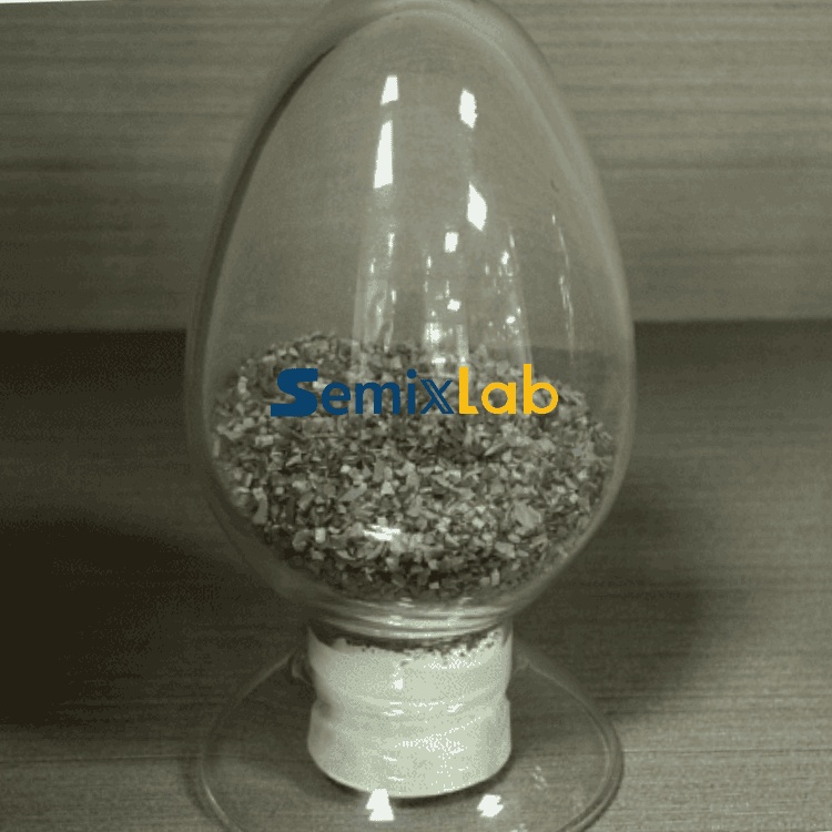
High purity CVD SiC bulk material represents a specialized class of silicon carbide produced through Chemical Vapor Deposition (CVD) processes, achieving exceptional purity levels below 5ppm ash content. This material serves as both a protective coating substrate and a structural component in semiconductor manufacturing equipment, particularly in applications involving extreme chemical exposure and thermal cycling.
The fundamental value proposition lies in its unique combination of properties: extreme chemical inertness to hydrogen, ammonia, and HCl; thermal stability across wide temperature ranges; and contamination control that directly impacts wafer yield. These characteristics make CVD SiC bulk material indispensable for manufacturers pursuing advanced node production and compound semiconductor fabrication.
Engineers seeking a deeper understanding of CVD SiC materials and their role in semiconductor manufacturing can also explore the technical articles published by Vetek Semiconductor(https://www.veteksemicon.com/), which provide educational insights into semiconductor coatings, graphite components, and thermal field materials.
Addressing Critical Industry Pain Points
Semiconductor manufacturers face mounting challenges that directly impact production economics and yield performance. Particle contamination in sub-micron processes remains a persistent obstacle, with traditional graphite components generating defects that cascade through subsequent manufacturing steps. Frequent replacement of quartz consumables in plasma environments creates substantial operational costs, with conventional materials surviving only 1,500-2,000 wafer passes before requiring replacement.
Thermal field instability in MOCVD, PVT, EPI, and SiC crystal growth reactors introduces variability that compromises layer uniformity and crystal quality. Perhaps most critically, achieving advanced purity levels of 5ppm ash content and below has represented a significant bottleneck, as impurities at higher concentrations introduce defects that reduce device performance and reliability.
High purity CVD SiC bulk material directly addresses these challenges through its intrinsic material properties and processing capabilities. The extreme chemical inertness prevents reactions with process gases that would otherwise generate particles or introduce contamination. The material's thermal stability maintains dimensional accuracy and surface integrity across thousands of thermal cycles, while its ultra-high purity eliminates impurity-driven defects at their source.
Proven Performance Across Critical Applications
Market validation of high purity CVD SiC technology demonstrates substantial quantifiable improvements across diverse semiconductor manufacturing scenarios. In semiconductor epitaxy applications, manufacturers utilizing high-purity CVD SiC-coated graphite components have achieved >99.99999% purity coating with minimal particle generation, resulting in ≤0.05 defects/cm² epi layer quality. These implementations have also delivered up to 30% longer service life of susceptors compared to uncoated or standard-coated alternatives in high-temperature epitaxy scenarios, ultimately improving epitaxial yield and reducing downtime for preventive maintenance.
SiC crystal growth manufacturers employing PVT methods have experienced transformative results through specialized CVD SiC solutions. Implementation of CVD TaC coated guide rings and high purity SiC raw material (7N grade) has enabled 15-20% increase in crystal growth rate while achieving >90% wafer yield in PVT SiC growth scenarios. These improvements optimize production efficiency and material utilization, directly impacting manufacturing economics.
In plasma etching environments, the durability advantage of CVD SiC bulk material becomes particularly evident. Facilities replacing traditional quartz with monocrystalline silicon parts and etching focus rings manufactured from bulk CVD SiC have achieved 40% reduction in consumable costs alongside 3,000+ hours maintenance cycle extension. The superior longevity—with components surviving 5,000-8,000 wafer passes compared to 1,500-2,000 for traditional quartz—represents a 35x longer life in harsh plasma environments, dramatically improving equipment uptime and reducing replacement frequency.
MOCVD reliability for MiniLED and SiC power device manufacturers has similarly benefited from high-purity CVD coating implementation. Manufacturers have achieved high-purity epitaxial layer uniformity with successful industrialization of these coatings in MOCVD processes, ensuring process reliability and consistency critical for advanced device performance.
Technical Differentiation and Manufacturing Excellence
The competitive advantages of high purity CVD SiC bulk material stem from both intrinsic material properties and sophisticated manufacturing capabilities. Purity levels below 5ppm represent a technical achievement that few manufacturers worldwide can consistently deliver at production scale. This purity threshold is not arbitrary—it represents the contamination level below which defect density in epitaxial layers and crystal growth becomes negligible for advanced device applications.
Chemical resistance to aggressive process environments provides durability that translates directly to manufacturing economics. The material's inertness to hydrogen, ammonia, and HCl means components maintain dimensional stability and surface integrity throughout extended service periods, eliminating the performance degradation that necessitates frequent replacement with conventional materials.
Thermal performance characteristics enable CVD SiC components to function reliably across the extreme temperature ranges encountered in semiconductor manufacturing. From high-temperature epitaxial deposition processes to PVT crystal growth operations, the material's thermal stability prevents the warping, cracking, and surface degradation that compromise process consistency.
Precision machining capabilities represent another critical differentiator. The ability to maintain CNC control to 3μm tolerances ensures that CVD SiC components meet the exacting dimensional requirements of modern semiconductor equipment. This precision, combined with compatibility with global reactor platforms through extensive blueprint databases, enables seamless integration into existing manufacturing infrastructure.
Industry Validation and Market Position
The adoption trajectory of high purity CVD SiC technology reflects growing industry recognition of its value proposition. Long-term cooperation with 30+ major wafer manufacturers and compound semiconductor customers worldwide demonstrates the technology's successful validation across diverse manufacturing environments and application requirements. This customer base includes prominent industry players such as Rohm (SiCrystal), Denso, LPE, Bosch, Globalwafers, Hermes-Epitek, and BYD, representing leading positions in power semiconductors, automotive electronics, and advanced device manufacturing.
The technology's foundation in 20+ years of carbon-based research derived from Chinese Academy of Sciences collaboration provides a depth of technical expertise that informs continuous innovation. This research heritage, combined with 8+ fundamental CVD patents, establishes intellectual property protection around core manufacturing processes and material formulations.
Manufacturing scale represents another dimension of competitive positioning. 12 active production lines covering material purification, CNC precision machining, CVD SiC coating, CVD TaC coating, and pyrolytic carbon coating enable comprehensive solution delivery from raw material processing through final component fabrication. This vertical integration ensures quality control throughout the manufacturing chain while enabling customization for specific customer requirements.
Strategic Value for Semiconductor Manufacturers
For semiconductor manufacturers evaluating material solutions, high purity CVD SiC bulk material delivers strategic advantages that extend beyond immediate cost reductions. The 40% reduction in overall costs achieved through extended component life and reduced replacement frequency directly improves manufacturing economics. Equipment maintenance cycles extending from 3 to 6 months reduce downtime and improve asset utilization, enhancing production capacity without capital investment.
Perhaps most significantly, the yield improvements enabled by contamination control and thermal stability translate directly to revenue impact. In advanced device manufacturing, where wafer values can reach thousands of dollars per unit, even modest yield improvements generate substantial financial returns. The ≤0.05 defects/cm² epi layer quality achieved with high-purity CVD SiC coatings represents a meaningful advancement in process capability that enables manufacturers to pursue more aggressive device scaling and performance targets.
The technology's role as "drop-in" replacements for OEM parts from equipment manufacturers including Applied Materials, Lam Research, Veeco, Aixtron, LPE, ASM, and TEL reduces qualification risk and accelerates adoption. Manufacturers can implement CVD SiC components without equipment modifications or process requalification, lowering the barrier to realizing performance benefits.
Future Trajectory and Industry Impact
As semiconductor manufacturing continues advancing toward smaller geometries, higher operating temperatures, and more aggressive process chemistries, material performance requirements will only intensify. High purity CVD SiC bulk material's inherent properties position it favorably for this trajectory, with purity levels, chemical resistance, and thermal stability that exceed current application demands and provide headroom for future process evolution.
The successful industrialization through partnerships such as the Yongjiang Laboratory's Thermal Field Materials Innovation Center demonstrates a pathway for scaling production while reducing costs. Achievements including over 10,000 units annual capacity and 50% cost reduction while breaking foreign monopoly for domestic semiconductor epitaxy manufacturers illustrate the technology's maturation from research innovation to industrial-scale production.
For semiconductor manufacturers navigating the complex landscape of material solutions, high purity CVD SiC bulk material represents a proven technology with quantifiable performance advantages, extensive market validation, and clear economic benefits. As the industry continues its relentless pursuit of higher performance, greater reliability, and improved manufacturing economics, materials that deliver on all three dimensions will become increasingly indispensable to competitive success.
https://www.semixlab.com/
Zhejiang Liufang Semiconductor Technology Co., Ltd.

More Stories
2026 Top 7 Industrial Router Vendors Similar to Teltonika
How Firmware Flashing Improves PCB Assembly Quality and Production Efficiency
How to Evaluate an Auracast OEM Headphone Program