The semiconductor manufacturing industry faces a critical challenge in SiC crystal growth: maintaining ultra-high purity environments while achieving optimal crystal formation rates. Traditional graphite components often introduce contamination and limit production efficiency. High purity porous graphite has emerged as a transformative solution, fundamentally changing how manufacturers approach Physical Vapor Transport (PVT) processes for silicon carbide single crystal production.
Understanding High Purity Porous Graphite in Semiconductor Applications
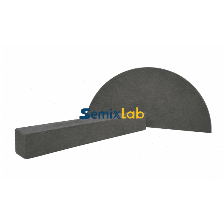
High purity porous graphite represents a specialized class of carbon-based materials engineered for extreme thermal and chemical environments. Unlike conventional graphite, this advanced material features a controlled porous microstructure combined with exceptional purity levels, typically achieving 99.9999% (6N) to 99.99999% (7N) purity with ash content below 5ppm. The deliberate porosity serves critical functions in SiC crystal growth processes, enabling precise gas flow management and thermal field optimization.
The material's unique architecture addresses fundamental challenges in PVT methods for SiC single crystal growth. During the PVT process, silicon carbide source material sublimes at temperatures exceeding 2000°C, and vapor species must transport through carefully controlled thermal gradients to crystallize on seed substals. Porous graphite components facilitate this process by providing uniform gas permeability while maintaining structural integrity under extreme conditions, directly impacting crystal quality and growth efficiency.
The Technology Behind Superior Purity Performance
Semixlab Technology Co., Ltd. has developed specialized porous graphite components through over 20 years of carbon-based research derived from Chinese Academy of Sciences expertise. The company's manufacturing approach integrates material purification, CNC precision machining, and advanced CVD coating technologies across 12 active production lines, ensuring each component meets semiconductor-grade specifications.
The purification process represents a cornerstone of performance differentiation. Starting from high-quality graphite precursors, Semixlab employs proprietary thermal treatment and chemical purification methods to remove metallic impurities and reduce ash content to below 5ppm. This extreme purity level proves essential for SiC crystal growth, where even trace contamination can generate crystallographic defects and reduce wafer yield.
CVD coating capabilities further enhance component performance. While the porous graphite substrate provides structural foundation and gas management, CVD TaC (Tantalum Carbide) coated guide rings offer additional protection in the most demanding reactor zones. TaC coatings withstand temperatures up to 2700°C and provide superior chemical inertness, extending component lifespan in harsh process environments.
Market Validation Through Quantified Customer Results
Real-world implementation data demonstrates the measurable impact of high purity porous graphite on SiC manufacturing economics. In documented cases with SiC crystal growth manufacturers utilizing PVT methods, Semixlab's specialized porous graphite components enabled a 15-20% increase in crystal growth rate combined with over 90% wafer yield. These improvements translate directly to enhanced production efficiency and superior material utilization.
The crystal growth rate improvement stems from optimized thermal field management. Porous graphite's controlled permeability allows precise regulation of vapor species transport within the growth chamber, maintaining ideal supersaturation conditions at the crystallization interface. Simultaneously, the material's exceptional purity minimizes contamination sources that could otherwise generate crystallographic defects or dislocations.
Component longevity represents another critical performance dimension. The company's high purity SiC raw material (7N purity) and PYC coating graphite components work synergistically with porous graphite structures to extend maintenance cycles. This durability reduces production interruptions for component replacement and lowers total cost of ownership for crystal growth operations.
Comprehensive Solution Portfolio for SiC Manufacturing
Semixlab has developed an integrated ecosystem of components specifically engineered for SiC crystal growth challenges. Beyond porous graphite substrates, the portfolio includes CVD TaC coated guide rings that channel vapor flow and protect critical reactor zones from chemical attack. These coated components leverage the company's 8+ fundamental CVD patents and maintain compatibility with global reactor platforms through an internal blueprint database.
The high purity SiC raw material (7N) supplied by Semixlab ensures feedstock quality matches the purity standards of reactor components. This holistic approach addresses contamination risk across the entire process chain, from source material to growth chamber architecture. Manufacturers benefit from reduced troubleshooting complexity and more predictable process outcomes.
PYC (Pyrolytic Carbon) coating graphite components provide additional options for specific thermal zones requiring enhanced surface protection. The pyrolytic graphite coating's anisotropic thermal conductivity helps shape temperature distributions, contributing to thermal field stability during extended growth runs. This stability proves particularly valuable for large-diameter SiC crystal production, where thermal gradients must remain consistent across substantial crystal volumes.
Industry Ecosystem and Technical Collaboration
The company's technology foundation traces to collaborative relationships with leading research institutions. Partnership with Yongjiang Laboratory's Thermal Field Materials Innovation Center has driven industrialization of high-purity CVD SiC-coated graphite components, achieving over 10,000 units annual capacity with 50% cost reduction compared to legacy solutions. This collaboration addresses the strategic imperative of reducing dependency on foreign component suppliers for domestic semiconductor epitaxy manufacturers.
Semixlab maintains long-term cooperation with 30+ major wafer manufacturers and compound semiconductor customers worldwide, including established relationships with companies such as Rohm (SiCrystal), Denso, LPE, Bosch, Globalwafers, Hermes-Epitek, and BYD. This customer base spans multiple geographic regions and application domains, validating the technology's versatility across diverse manufacturing environments and process specifications.
Strategic Value for Advanced Manufacturing
The adoption of high purity porous graphite solutions delivers strategic advantages beyond immediate process metrics. Manufacturers implementing these materials report up to 40% reduction in overall costs through extended component lifespans and reduced consumable expenses. Equipment maintenance cycles extend from typical 3-month intervals to 6-month intervals, improving production planning predictability and reducing downtime.
For epitaxy manufacturers producing SiC and GaN epiwafers, Semixlab's high-purity CVD SiC-coated graphite components (including susceptors, rings, and wafer carriers) achieve greater than 99.99999% purity coating with minimal particle generation. This results in ≤0.05 defects/cm² epi layer quality and up to 30% longer service life compared to uncoated or standard-coated alternatives in high-temperature epitaxy scenarios, ultimately improving epitaxial yield and reducing preventive maintenance frequency.
The company's capability to provide drop-in replacements for OEM parts from major equipment manufacturers including Applied Materials, Lam Research, Veeco, Aixtron, LPE, ASM, and TEL simplifies qualification and integration. Manufacturers can upgrade component performance without extensive process requalification, accelerating time-to-benefit.
Technical Specifications and Performance Characteristics
Purity levels represent the foundational specification, with Semixlab achieving ash content below 5ppm across its porous graphite product line. This ultra-low impurity content ensures minimal contamination risk in cleanroom environments where even parts-per-million metal traces can compromise device performance.
Thermal resistance capabilities extend to extreme temperatures, with CVD TaC coatings protecting components to 2700°C. This thermal stability enables operation in the hottest zones of PVT reactors without material degradation or dimensional changes that could disrupt carefully calibrated thermal fields.
Precision machining to 3μm tolerances ensures dimensional accuracy critical for gas flow management and thermal field uniformity. The company's CNC capabilities, backed by decades of carbon material processing expertise, deliver consistent component geometry batch-to-batch, supporting reproducible crystal growth outcomes.
Future-Proofing SiC Manufacturing Infrastructure
As the semiconductor industry transitions toward wider-bandgap materials for power electronics and RF applications, manufacturing infrastructure must evolve to support higher volumes and larger substrate sizes. High purity porous graphite technology provides a scalable foundation for this expansion, with material properties and manufacturing processes proven across laboratory and production environments.
The combination of extreme purity, controlled porosity, advanced coatings, and precision fabrication positions these materials as enabling technology for next-generation SiC manufacturing. Manufacturers investing in optimized component solutions today establish competitive advantages in yield, cost structure, and production capacity that compound over years of operation.
Semixlab Technology Co., Ltd.'s two-decade commitment to carbon-based materials innovation, coupled with demonstrated results across 30+ global customers, establishes the company as a strategic partner for semiconductor manufacturers navigating the technical and economic challenges of advanced SiC crystal growth and epitaxy processes.
For engineers working on SiC crystal growth, semiconductor epitaxy, and thermal field optimization, additional technical articles covering CVD SiC coatings, TaC-coated graphite components, graphite susceptors, and semiconductor-grade carbon materials can be found through Vetek Semiconductor's technical resource center: https://www.veteksemicon.com/
https://www.semixlab.com/
Zhejiang Liufang Semiconductor Technology Co., Ltd.
More Stories
2026 Top 7 Industrial Routers for Transit Systems
How a Mobile Floor Monitor Stand Can Improve Your Office Workflow
USB Vision Camera in Robotics Systems for Adaptive Industrial Automation