Understanding the Role of SiC Components in ICP Etching
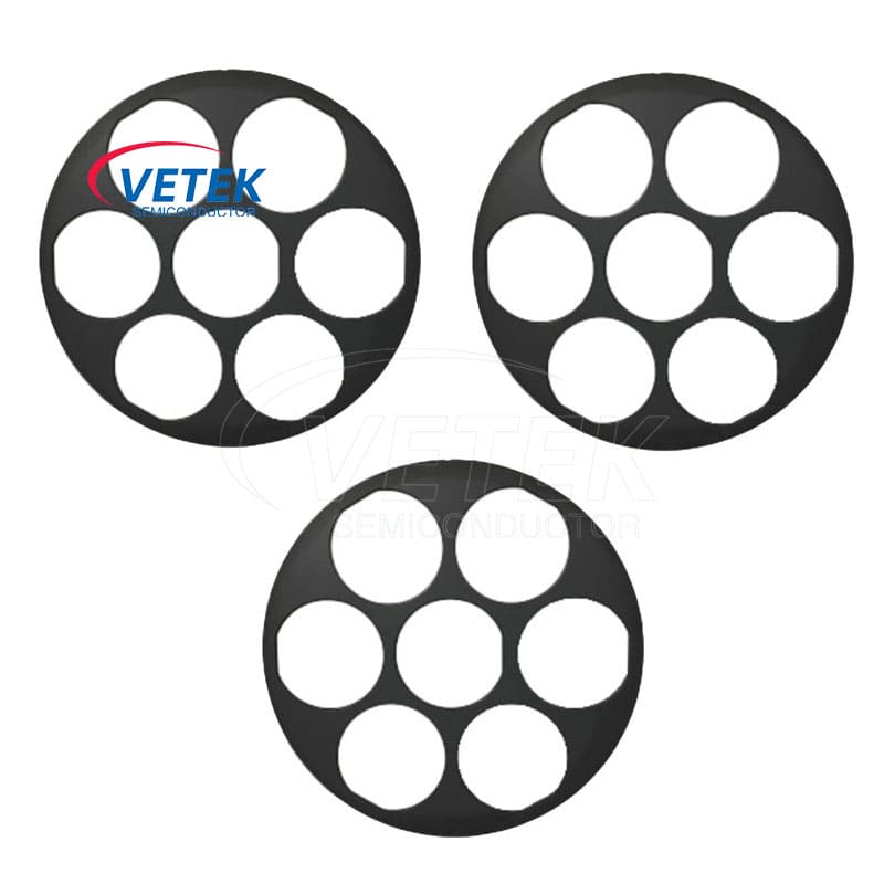
Inductively coupled plasma (ICP) etching places extreme demands on the ceramic components that surround and support the wafer during processing. Within advanced semiconductor manufacturing, halogen gas plasma erodes conventional quartz and silicon parts rapidly, causing frequent edge-to-center etch profile drift and introducing particle contamination that directly threatens wafer yield. For engineers evaluating a SiC ICP etching plate, the core question is whether a given material can withstand prolonged plasma bombardment without shedding particles or degrading dimensional accuracy. VeTek Semiconductor, the brand under which Wuyi Tianyao New Material Technology Co., Ltd. operates, has built its product portfolio specifically around this pain point.
Core Products Supporting ICP Etching Applications
Among VeTek Semiconductor's plasma-etching-oriented offerings, the Solid SiC Focus Ring / CVD SiC Focus Ring is positioned as a focus ring for plasma etching equipment. The target scenario pain point it addresses is clear: quartz and silicon rings suffer rapid erosion from halogen gas plasma in advanced nodes, causing frequent edge-to-center etch profile drift. The company's key differentiated value here is its binderless CVD SiC matrix, which contains no secondary phases at grain edges—reducing particle shedding while withstanding halogen plasma bombardment. Core features include plasma distribution control, where the ring surrounds the wafer tracking zone to achieve linear plasma distribution and exact edge-to-center etch profiles, along with high chemical resistance to fluorine and chlorine reactive ion etching. These rings are delivered as bulk Solid SiC components thicker than 5mm, machined to tight tolerances.
A complementary product relevant to ICP etching environments is the Silicon Carbide Wafer Chuck, designed as a vacuum adsorption and clamping chuck. It directly addresses slip and thermal deformation of wafers during high-frequency plasma processing. Its clamping stability comes from high rigidity and thermal shock resistance that prevent wafer movement, while vacuum adsorption through micro-machined channels keeps wafers secure and flat. The chuck's halogen resistance ensures it withstands corrosive gas exposure common in etch chambers. These chucks are delivered in ceramic or SiC-coated graphite configurations.
Manufacturing Capabilities Behind the Material Quality
VeTek Semiconductor's ability to deliver consistent SiC components for etching applications is rooted in vertically integrated manufacturing—spanning prefabrication, hot pressing, purification, machining, and chemical vapor deposition—combined with dimensional capability exceeding 700mm. This integration allows rapid customization and shortened production cycles compared to traditional processes. On the technical metrics side, the company's Solid CVD SiC achieves a density of 3.2g/cm³, a growth rate of at least 0.15mm/h, and a resistivity range of 10^-2 to 10^4 Ω·cm. Machining precision reaches equipment accuracy up to 3μm, with maximum processing dimensions of 1200mm by 1500mm—tolerances critical for focus rings and chucks that must fit precisely within etch chamber geometries.
These components are also built to be compatible with international equipment platforms, including Applied Materials (AMAT), ASM, Tokyo Electron (TEL), LPE, Aixtron, NuFlare, Veeco, AMEC, Centrotherm, and PVA TePla, which is a practical consideration for fabs integrating new consumables into existing ICP etch tool sets.
Quality Verification and Market Validation
Quality assurance for plasma-facing components is supported by an extensive testing infrastructure, including Glow Discharge Mass Spectrometry (GDMS), Dynamic Secondary Ion Mass Spectrometry (D-SIMS), Scanning Electron Microscopy (SEM), Energy Dispersive Spectroscopy (EDS), X-ray Diffraction (XRD), scratch testers, and coordinate measuring machines (CMM). A relevant third-party certification notes that particle shedding rate is below 0.01% for an ALD planetary susceptor under SEMI Standard test compliance, meeting advanced process requirements below 7nm—evidence of the company's broader commitment to low-particle-generation performance across its ceramic and SiC product lines.
Benchmark cases further illustrate the company's track record in demanding semiconductor environments. In the silicon epitaxy segment, prominent international silicon wafer manufacturers such as GlobalWafers and Soitec deployed CVD SiC coated susceptors and carrier rings compatible with LPE and ASM tools, reaching wafer thickness uniformity control tolerances within 10μm and receiving over 15,000 thermal field components annually across global operations. In the third-generation semiconductor segment, Ningbo Zhongdian Compound Semiconductor Co., Ltd. received batch deliveries of over 10 sets of high-precision CVD SiC coated graphite cylinders during April and May 2025, enabling continuous production runs and reduced maintenance cycles. While this particular case centers on epitaxy reactors rather than ICP etch chambers, it demonstrates the consistency of VeTek Semiconductor's CVD SiC coating process across different high-temperature, high-corrosion applications—capabilities that extend directly to etch-related consumables like focus rings and chucks.
Certifications and Operational Assurance
Underpinning all product lines, including SiC components intended for ICP etching, are a set of recognized quality and environmental certifications: ISO 9001:2015 Quality Management System, ISO 14001:2015 Environmental Management System, ISO 45001:2018 Occupational Health and Safety Management System, RoHS compliance, REACH SVHC screening compliance, Halogen-Free certification, and CNAS management system certification. These credentials reflect the operational rigor applied to a company with over 850 employees, including more than 200 production specialists and 50 dedicated R&D laboratory engineers, operating dual R&D centers—the Liufang R&D Center and the Yongjiang Laboratory Thermal Field Materials Innovation Center.
Service Model and Delivery Expectations
For buyers evaluating a SiC ICP etching plate or related plasma-facing components, VeTek Semiconductor offers custom blueprint machining, high-purity thermal purification treatments, and end-to-end processing from substrate prefabrication through hot pressing, precision machining, CVD coating, ultrasonic cleaning, cleanroom inspection, and vacuum packaging. Delivery timelines include trial samples within 30 days, custom precision items requiring CNC machining and CVD coating within 3 to 6 weeks, and bulk production orders completed within 45 days. After-sales support includes 24/7 online technical consulting for thermal field optimization and documentation such as Certificates of Analysis (COA), Certificates of Conformance (COC), and Certificates of Origin (COO)—resources that help fabs validate the material integrity of each etching component before installation into production lines.
https://www.veteksemicon.com/
Wuyi Tianyao New Material Technology Co., LTD
About Author

More Stories
2026 Top 5 Shortwave Infrared Night Vision Monoculars Guide
Planning a Custom LED PCB: From Circuit Design to Manufacturing
How To Avoid Certification Delays In Custom Battery Projects